Why DGX H100 NVL256 Never Shipped? Analysis of BoM, Will GB200 NVL72 Fail too?
DGX H100 NVL256/GH200 NVL256 Got Discontinued, GH200 NVL32 Re-Design, GB200/B200 NVL36/NVL72 Copper Analysis
NVIDIA's DGX H100 NVL256 and DGX GB200 NVL256, a supercomputing powerhouse that combined 256 NVIDIA H100 GPUs, never made it to market. Its absence has sparked discussions about why a high-capacity solution would be halted in development. The prevailing theory points to an insurmountable cost-to-benefit ratio. The extensive use of fiber optics to interconnect such a large number of GPUs significantly raised the Bill of Materials (BoM), driving the cost beyond what standard NVL8 configurations could justify.
DGX H100 NVL256 Superpod: AI Exascale
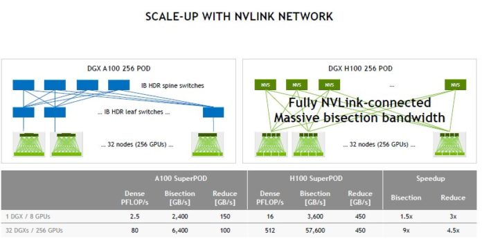
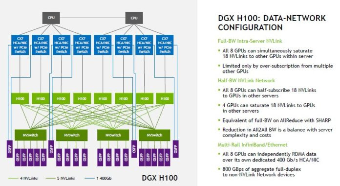
With scale-out NVL256, NVIDIA claims they can achieve 2x greater throughput for 400B MoE training, but large customers can done the math and found their claim to be questionable given the increased cost associated with getting NVL256. The latest generation NDR Infiniband is about to achieve 400Gbit/s while NVLink4 achieves 450Gbyte/s. So approximately a ~9x speed up on peak marketed bandwidth. It uses 128 L1 NVSwitches + 32 L2 External NVSwitches, which means there is a 1:2 blocking ratio and each server can only half subscrible to another each server. They related on NVlink SHARP in network reductions to get equivalent of full all2all Bandwidth on all-reduce.

H100 NVL256 BoM Analysis
Disclaimer of Unit price of each item will be from publicly available sources + adjustment to account for NVIDIA margins + volume discounts. We see that the addition of scale-out NVLink256 causes the BoM price to increase ~30% for each SU.
the 30% of the total cost of NVL256 stays constant all the way up to 2048 H100s. After 2048, it gets slightly lowered as the Infiniband cost percentage increases as we switch from a 2-tier Infiniband network topology to a 3-tier Infiniband network topology using a super-spine.
Major customers and hyperscaler did the perf/TCO analysis for their current workloads and found that spending 30% cost premium on additional HGX H100 servers had better perf/TCO compared to paying for NVL256 scale-out Nvlink. This caused NVIDIA to never ship DGX H100 NVL256 nor DGX GH200 NVL 256.
GH200 NVL32 Re-Design
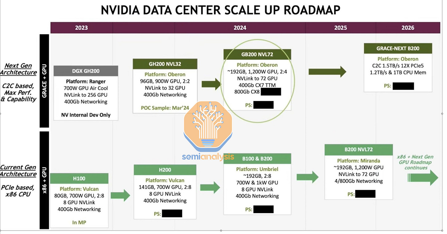
Thus caused NVIDIA to redesign NVL256 into just NVL32 using a copper backplane “spine” similar to their NVL36/NVL72 Blackwell design. AWS has agreed to purchase 16k GH200 NVL32. for their Project Ceiba.
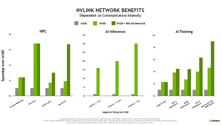
We estimate the price premium of this re-design NVL32 will be 10% over standard premium only HGX H100 BoM. Furthermore, workloads have kept getting larger and larger today compared to when hyperscalers were choosing HGX H100 NVL8 and NVL256. For GPT-3 175B with 16k GH200, NVIDIA claims NVL32 will have a 1.7x speed increase over 16k H100 and have 2x increase in 500B LLM inferencing. These perf/TCO is much more attractive to customers and we see that order of magnitudes more customers engaging with NVIDIA when they switched to a copper “spine” design.
Will GB200 NVL36/NVL72 Fail too?
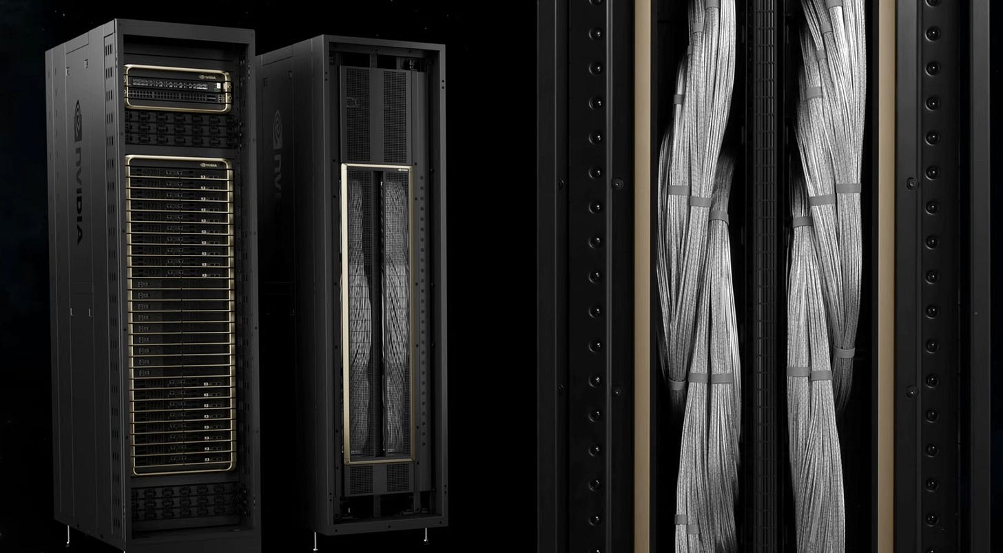
The anticipated launch of the GB200 NVL72 is different. It is believed that NVIDIA has learned from the H100 NVL256's failure, addressing cost concerns by adopting copper interconnects instead of relying solely on fiber optics. NVIDIA calls this copper interconnect “NVLink Spine”. This shift in design is expected to reduce the cost of goods (COG), suggesting that GB200 NVL72 could be on a successful path where its predecessor faltered.
NVIDIA claims that with this copper design, NVL72 will cost ~6x cost and save ~20kW per GB200 NVL72 rack and ~10kW per GB200 NVL32 rack.
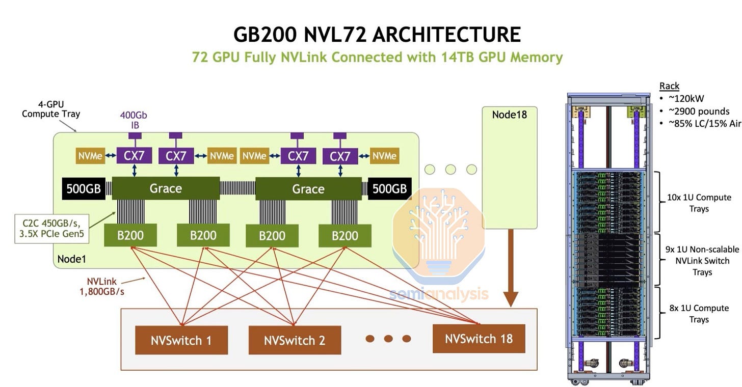
Unlike H100 NVL256, GB200 NVL72 will not have any NVLink Switch within the compute node as it rather opts for a flat rail-optimized network topology. For each 72 GB200 GB200s, there are 18 NVLink Switch. Since each connection is within the same rack, the farther connection only needs span 19U. Each U is 44.4mm, so 19U is 0.83metres, which is well within range for active driven copper.
Furthermore, NVIDIA claims, it can support up to 576 GB200 within a single Nvlink domain. This is probably done by an additional tier of Nvlink Switches. We believe that NVIDIA will keep this ratio of 1:2 blocking ratio, that means within a GB NVL576 SU, it would use 144 L1 NVLink Switch + 36 L2 NVLink Switch. Or they can move towards a more aggressive 1:4 blocking ratio by only using 18 L2 NVLink Switch. They will continue to use optical OSFP transceivers to scale from the L1 NVLink Switch within a rack to the L2 NVLink Switch.
NVL36 & NVL72 is rumoured to already made up more than 20% of NVIDIA’s Blackwell deliveries. But it is questionable if major customers would opt for the more expensive NVL576 due to the additional cost associated with requiring optics to scale to NVL576. It seem that NVIDIA has learned their lesson that passive copper and active copper is way more cheaper than optics.


